Posted on

Preparing Metal Thin Film Electrodes for ATR-SEIRAS

ATR-SEIRAS exploits the near-field interaction between incident infrared radiation and a thin metal film electrode, often a layer of gold. Working in the Kretschmann configuration, the surface of the metal layer can be probed under a variety of electrochemical conditions.

But how are metal layers for ATR-SEIRAS prepared? This post will describe the two main fabrication methods, physical vapour deposition and chemical (electroless) deposition. It will also describe a newly-developed method for preparing mechanically stable hybrid gold films using electrodeposition.

A general observation in ATR-SEIRAS is that metal films have very poor mechanical stability. Because of the poor adhesion of gold on silicon oxide surfaces, film delamination is the dominant failure mode. Metal films prepared by vapour or electroless should be handled very carefully. Prolonged potential excursions into gas evolution (highly anodic or cathodic potentials) will often result in high film stresses which contribute to failure.

Physical Vapour Deposition

Physical Vapour Deposition (PVD) methods generally use magnetron sputtering or thermal evaporation systems. Metal thin films in the 10 to 20 nm thickness range are deposited at low rates (typically around 0.01 nm/s) on the basal plane of an internal reflection element. The low deposition rate and thickness provide a rough surface with an island structure which is known to contribute favourably to signal enhancement.

From a practical standpoint, PVD methods are relatively quick and usually highly repeatable with a well-maintained system. Because the films are prepared in vacuum, it often takes several hours to pump the substrates down to base pressure. Deposition usually takes under an hour. Most PVD chambers can accommodate multiple substrates, allowing several metal layers to be prepared in parallel. This is particularly beneficial when using our microgrooved wafers, available for purchase in our web store.

Although metal deposition with PVD methods is relatively quick and easy, the layers can be less mechanically stable than those prepared with chemical (electroless) methods. In our experience, enhancement factors are often slightly lower as well.

Chemical (Electroless) Deposition

Electroless deposition using gold on a silicon substrate was first described by Osawa in 2002, and involves a series of mechanical and chemical steps. Compared to PVD, it is highly challenging and potentially hazardous, but results in robust films with good enhancement factors. The basal plane of the internal reflection element is first mechanically polished with diamond suspensions (decreasing to sub-micron particle sizes) then treated with HF to remove the native oxide layer and hydrogen terminate the surface. Then, a plating solution containing a gold precursor (often gold tetrachloroaurate) is introduced and allowed to react for one to two minutes before the reaction is quenched by rinsing with water.

We find that in the hands of a skilled practitioner, this method generates relatively robust films with strong enhancement. However, even an experienced user will only have about a 50% success rate. Furthermore, the highly corrosive solutions involved require extreme care in use and should be treated with appropriate caution. Deposition in this manner can only be performed one crystal at a time. In total, including preparation and cleanup, electroless deposition usually takes around two hours to complete.

Another option that has been reported in the literature is electroless deposition on ZnSe internal reflection elements. PIKE Technologies offers ZnSe face-angled crystals which are compatible with our JxF-series cells should you wish to try this.

Because of the difficulty and chemical hazards involved, new users should strongly consider avoiding electroless deposition if they have the resources to do so.

Hybrid Metal / Conductive Metal Oxide Films

JackfishSEC workers have recently demonstrated the preparation and use of hybrid films for ATR-SEIRAS. In Andvaag et al., a 50 nm film of indium zinc oxide (IZO) was deposited by magnetron sputtering and then gold nanoparticles were electrodeposited in the presence of a shape-directing ligand (4-methoxypyridine). Such films have remarkably high enhancement and are robust enough to withstand repeated potential cycles into hydrogen evolution. The paper linked above illustrates the stability of the hybrid film by reductively desorbing a thiol monolayer three times from the same film with no meaningful change in the spectrum quality. This is essentially impossible on a conventional gold film.

Hybrid films, which can also use indium tin oxide (ITO), require access to a PVD chamber to prepare the conductive metal oxide (CMO) layer. Electrodeposition can be completed in situ in a spectroelectrochemical cell so that the enhancement can be monitored during the process. Although multiple CMO layers can be deposited in parallel, electrodeposition takes place in series, although it takes only around an hour to complete.

“Activating” A Metal Layer

Most of the literature describes a potential cycling routine to “activate” the metal layer. The exact processes involved are still unclear, but the empirical result is that the signal enhancement increases during the process. This will be covered in detail in a future post.

Posted on

Optimal Angle of Incidence for ATR-SEIRAS

The enhancement factor for ATR-SEIRAS depends on both the polarization and the angle of incidence (AOI) of the light through the internal reflection element (IRE). Furthermore, the AOI providing maximum enhancement, AOImax, depends on the morphology of the metal film. For films of contiguous metal islands, such as those typically formed from both the electroless and physical vapour deposition methods cited in the literature, AOImax is close to 70-80° (all angles measured from the surface normal). For films composed of more isolated metal islands, AOImax is closer to the critical angle for total internal reflection. Having the JF cell mounted on a variable angle instrument, such as PIKE’s VeeMAX 3, is very convenient for determining AOImax for a particular configuration. Many of the additional considerations for selecting the optimal angle of incidence are described by Sigrist et al (Applied Spectroscopy. 2019, 73, 1394-1402).

When selecting the AOI on the ATR accessory, one must also consider the effects of refraction at the air/IRE interfaces. In other words, the AOI setting on the accessory does not necessarily equate to the effective AOI (AOIeff) through the internal reflection element. When using a curved surface IRE, such as a Si or ZnSe hemisphere, the value of AOI remains unperturbed by the the air/IRE interface as infrared light should be normally incident on the crystal surface. However, in the case of face-angled crystals, or microgrooved wafers, refraction should be considered.

Below is a simple widget that will allow the calculation of AOIeff through a crystal of known refractive index and face angle.

Posted on

External versus Internal Reflection Techniques

Wondering what the difference is between external and internal reflection techniques for infrared spectroelectrochemistry? Read on for a short introduction and to learn why ATR-SEIRAS is our technique of choice for surface-sensitive measurements.

Studying the molecular composition of the boundary between two materials, such as an electrode|electrolyte interface, is an inherently challenging problem due to the relatively small numbers of molecules at a surface compared to those in a bulk phase. Mechanisms that preferentially increase surface molecule sensitivity are highly desirable for such studies and there are two limiting approaches for surface enhanced infrared spectroelectrochemistry.

External Reflection

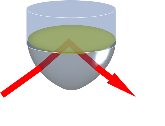
Schematic of external reflection spectroelectrochemistry with an infrared transparent crystal and thin layer of solution.
External reflection geometry. Infrared radiation is transmitted through a crystal and reflects off an electrode which is pushed close to the crystal.

In external reflection techniques, a highly polished metal electrode is pushed close to a suitably IR-transparent crystal forming a thin (ca. 10 µm) pocket of electrolyte. IR light transmitted through the crystal, reflects from the metal surface and is sent to the detector.

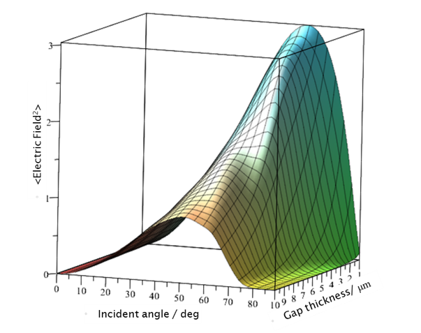
A graph of electric field enhancement versus incident angle and gap thickness.
In external reflection, the electric field distribution is easily quantified as a function of angle of incidence and gap thickness between the crystal and electrode. Overall surface enhancement is very low.

Upon reflection at the metal-solution interface, the electric field of p-polarized light undergoes a 180° phase shift whereas s-polarized light does not. Thus, at the interface, a theoretical enhancement factor, (E/Eo)2= 4, can be generated for p-polarized light (see Figure below). The contribution of solution based species to the measured p-polarized absorbance can be removed by subtracting the equivalent measurement made with s-polarized light. External reflection methods are often performed with either static wire grid polarizers (SNIFTIRS : subtractively normalized interfacial Fourier Transform Infrared Spectroscopy) or rapidly electromodulated crystals (PM-IRRAS : polarization modulation infrared reflection absorption spectroscopy).

Advantages

  • electric field distribution at the interface can be accurately calculated
  • quantitative information on surface concentrations and molecular orientation can be extracted

Disadvantages

  • low surface enhancement factor (up to 4)
  • infrared light has to pass through the highly absorbing electrolyte solution

Internal Reflection

ATR-SEIRAS (attenuated total reflection surface enhanced infrared absorption spectroscopy) in an internal reflection technique that overcomes the problems associated with solvent absorption. In ATR-SEIRAS a high refractive index internal reflection element (IRE) such as ZnSe, Ge or Si is modified by a thin film of nano-textured metal. As is the case in ATR, an evansecent wave is generated at angles above the crtical angle and this evansecent wave is coupled into localized plasmon polariton modes of the metallic film.

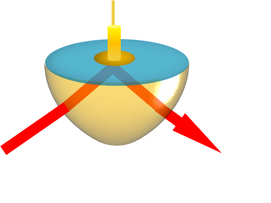
Schematic of ATR-SEIRAS, an internal reflection technique, with an infrared transparent crystal and a textured metal film.
ATR-SEIRAS, an external reflection, overcomes the strong IR absorption of the electrolyte by exploiting total internal reflection of IR radiation off a plasmonic metal film. ATR-SEIRAS can generate enhancement factors of up to 100x.

In simplistic terms, ATR-SEIRAS is analogous to its vibrational cousin SERS although it is important to note that surface enhancement in ATR-SEIRAS can be generated at almost all metals (see forthcoming note on the ATR-SEIRAS mechanism). Unlike external reflection methods, the enhancement is highly localized to the very surface of the metal and, as a good rule of thumb, the electric field enhancement drops off very rapidly beyond distances greater than 5-10 nm from the metal surface.

Advantages

  • High surface enhancement factors (up to 100)
  • Excellent surface sensitivity
  • Not limited to plasmonic metals

Disadvantages

  • Surface enhancement factors are hard to quantify
  • Metal film preparation can be difficult

The Jackfish SEC J1 and J1W spectroelectrochemical cell is an out of the box solution for performing ATR-SEIRAS measurements with the PIKE VeeMAX III variable angle accessory. Check our Products page for more information.